Electronic Devices
Electronic Devices
The purpose of this is to give quick reference to information or to use in an emergency (like if your text has accidentally been left under your desk at school).
This is NOT intended to replace reading the text with its excellent photographs, diagrams, charts, and tables.
ELECTRONIC DEVICES
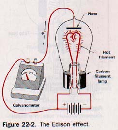
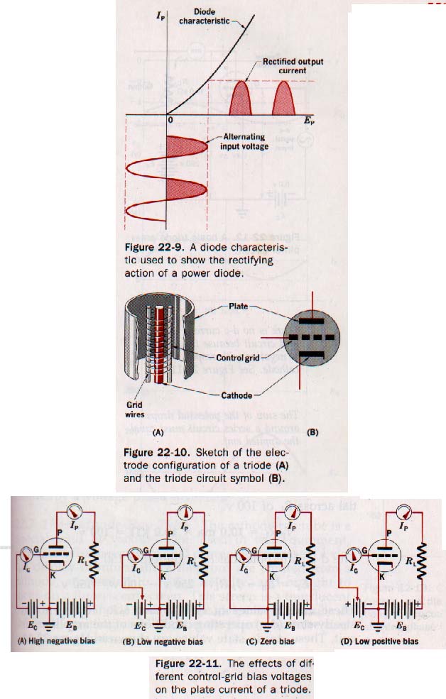
Vacuum Tubes: The Edison Effect is the boiling off of electrons from a heated filament. This is Thermionic Emission.
The Triode has a control grid between the cathode and the anode (plate). Varying the charge in the grid, controls the current flow through the tube.
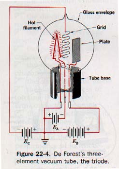
The Triode Amplifier uses the control grid to reproduce a weak signal as a strong output.
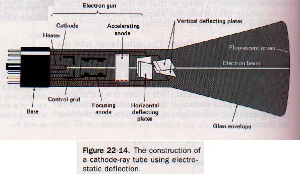
The Cathode Ray Tube uses charges to deflect the beam of electrons onto a fluorescent screen.
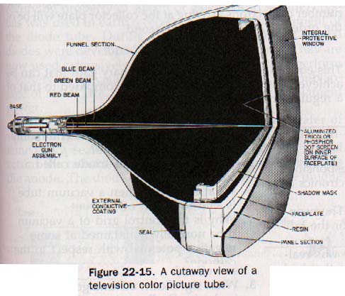
The Television Tube uses electromagnets to deflect the electron beams. Three beams actuate the three primary colors of phosphors on the screen.
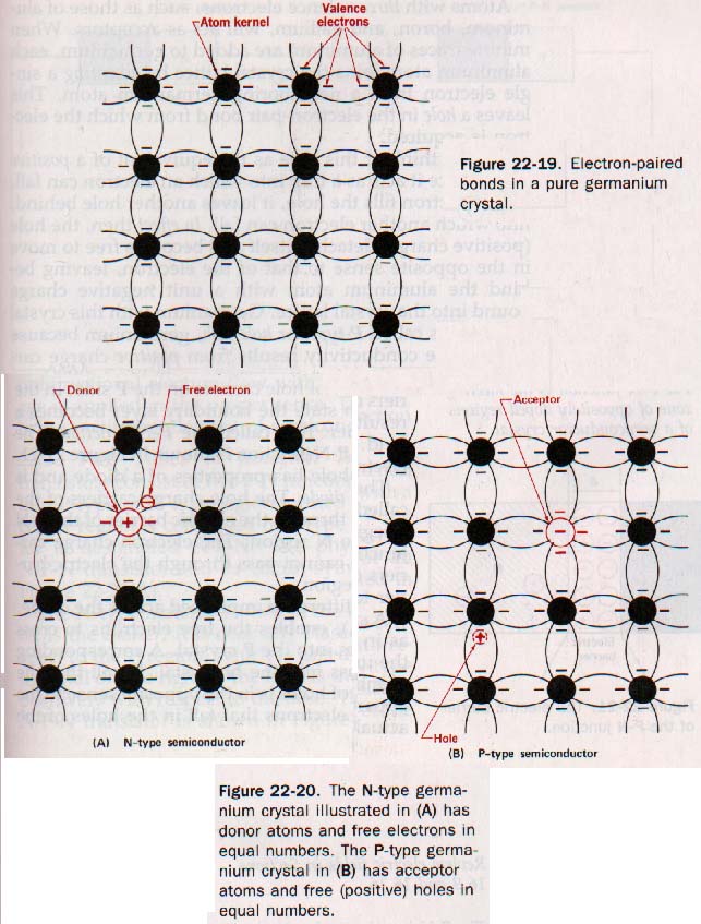
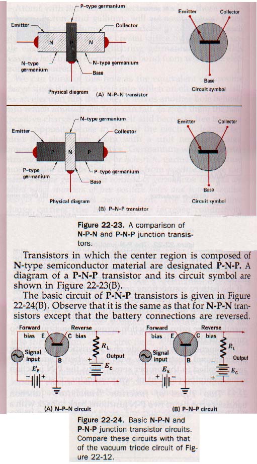
Transistors use n p type semiconductors. N-type use electrons to carry current, P-type use positive "holes" to carry current.
SUMMARY
High-vacuum tubes are identified as diodes, triodes, tetrodes, and pentodes based on the number of electrodes present. Low-vacuum tubes contain a gas under reduced pressure.
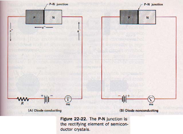
Diodes are used as detectors for radio signals and as rectifiers for converting alternating current to direct current. They are classed as signal or power diodes.
Electrons are emitted from the cathode of a vacuum tube by a process of thermionic emission. Electron emission is a function of emitter temperature. Emitters can be either directly or indirectly heated. Voltage and power amplification are possible in triode circuits because a small signal on the grid circuit is capable of controlling a large current in the plate circuit. Conduction in a vacuum tube results from the thermionic emission of electrons from the cathode and the attraction of the electrons to the positively charged plate.
The tube bias voltage between the control grid and the cathode establishes the operating condition of the tube. Bias voltages are produced by three methods. The a-c voltage gain across a vacuum-tube amplifier is accompanied by a voltage phase inversion .
P- and N-type semiconductors are formed by doping with trace quantities of acceptor and donor atoms respectively. N-type semiconductors are electron-rich materials. The free electrons are the negative charge carriers. P-type semiconductors are hole-rich materials. The holes act as positive charge carriers.
The P-N junction acts as an electric barrier in the meeting zone of oppositely doped regions of a semiconductor crystal. The direction of the electric field across the junction is from the N side to the P side.
Junction transistors consist of two P-N junctions back to back with thin P or N regions in between. They are designated N-P-N and P-N-P. Transistor elements correspond functionally to the elements of a vacuum triode.
In transistor circuits the emitter has a forward-bias voltage and the collector has a reverse bias voltage. Three circuit configurations are used: common base, common emitter, and common collector.
The transistor is a current-operated device. The amplifying property is the result of current changes that occur in the different transistor regions when proper voltages are applied to the transistor elements. The performance of a transistor is indicated by its family of characteristic curves. The forward current gain of a common-base configuration is called its alpha characteristic.
It is the ratio of the change in collector current to the change in emitter current for a constant collector-to-base voltage. The current gain of a common-emitter configuration is called its beta characteristic. It is expressed as the ratio of the change in collector current to the change in base current for a constant collector-to-emitter voltage.
The photovoltaic effect can provide the direct conversion of radiant energy to electric energy. Photovoltaic action is a type of photoelectric effect. The solar cell is a semiconductor diode in which the semiconductor crystal is doped in a special way. The construction and P-N junction provide the energy conversion effect when light strikes the cell's surface.
VOCABULARY
acceptor elemen, amplifier, base, cathode-ray tube, collector, cut-off bias, diode, donor, element doping, Edison effect, electronics, electron-rich, semiconductor, electrostatic lens, emitte,r forward bias, hole-rich, semiconductor, N-P-N transistor, N-type semiconductor, photovoltaic effect, P-N junction, P-N-P transistor, P-type semiconductor, rectifier, reverse bias, secondary emission, solar cell, space charge, thermionic emission, transistor, triode
Ah Yaz Indeed!
 Assignment Sheet for this Research Text Only.
 Go to Textbook Assignments for Portfolio:
.................................First Semester
.................................Second Semester